
Stackable Solar Panels
Increasing Power Density
Enkara’s Stackable Solar Panels are designed to increase power density by allowing multiple complementary photovoltaic modules to be integrated within the same footprint vertically. Using advanced thin‑film engineering and transparent semiconductor structures, these modules create new opportunities for high‑value solar deployment where surface area is constrained and higher output is essential.
A New Class of Thin‑Film Solar Architecture
Traditional solar modules rely on a single semiconductor absorber layer optimized for direct sunlight at a fixed orientation. This limits total energy generation per square meter and creates diminishing returns when installation space is limited.
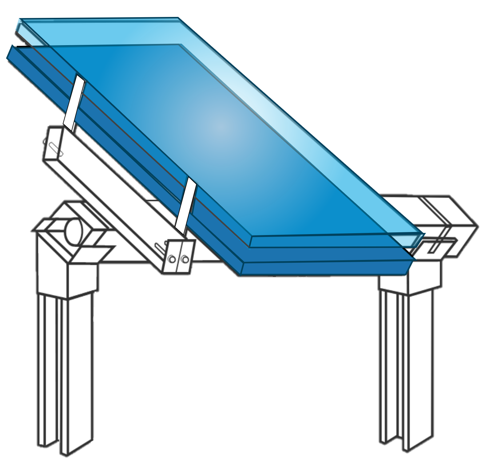
Enkara’s stackable architectures solve this problem by pairing multiple, optically compatible photovoltaic layers each tuned to different parts of the solar spectrum. Similar to 4-Termainl Tandem Solar Cells, these are mechanically separable and electrically distinct layers, which operate as vertically separated solar arrays, generating more energy from the same physical area without the electrical manufacturing constraints of traditional tandem solar devices.
Overcoming the Limitations of Silicon
Silicon‑based solar cells can capture roughly one‑third of the sun’s energy, and after decades of development the technology is approaching its physical limits for further efficiency gains. This creates diminishing returns even with incremental improvements, a single silicon layer cannot harvest the majority of usable sunlight, and performance falls sharply when the panel is not perfectly angled toward the sun. These constraints are especially problematic in installations where space is limited or where the solar surface cannot be optimally oriented, leaving a large portion of the spectrum, and potential power, unutilized.
Combining CdTe with Silicon
For decades, researchers and companies have attempted to combine cadmium telluride (CdTe) and silicon into a single high‑efficiency tandem solar cell, but the two materials are fundamentally incompatible when grown or manufactured together. Differences in current, voltage, lattice structure, thermal expansion, chemical behavior, and deposition methods made integrated CdTe‑on‑silicon devices unstable, inefficient, or impossible to produce at scale. Enkara’s approach avoids these historical challenges entirely. By using mechanically stacked layers that remain electrically separate, the CdTe and silicon cells each operate at their optimal performance without interfering with one another. This architecture preserves the strengths of both materials, eliminates the integration problems that have prevented progress for decades, and enables a practical path to higher power density in excess of 40% conversion efficiency.
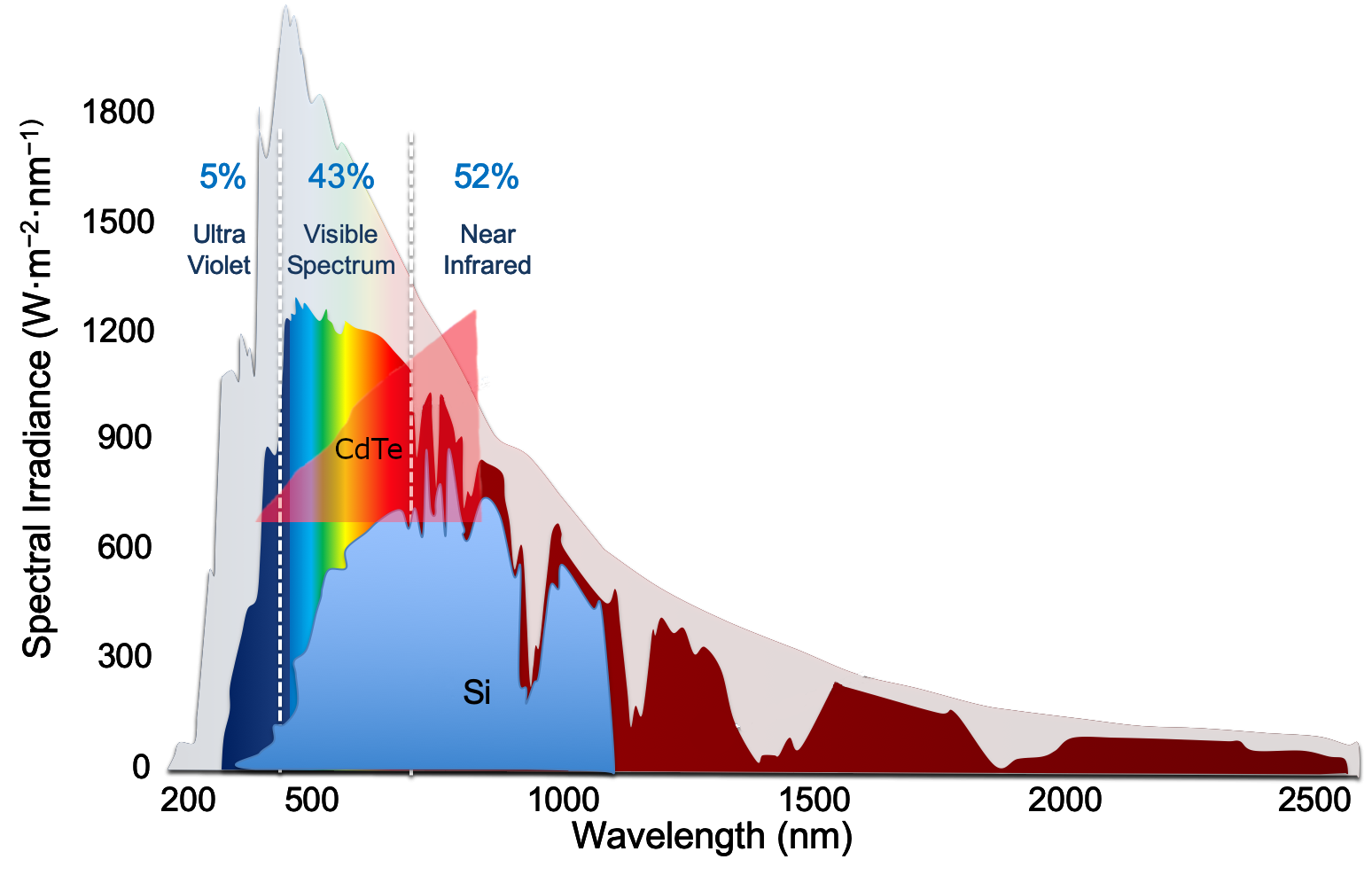
The combined absorbance spectrum of silicon and cadmium-telluride photovoltaic materials.